Lattice LC4256V-75TN100C: A Comprehensive Technical Overview of the CPLD Architecture and Application
The Lattice LC4256V-75TN100C represents a specific implementation within Lattice Semiconductor's mature ispMACH 4000V CPLD family. This device encapsulates the core strengths of Complex Programmable Logic Devices (CPLDs), offering a blend of high performance, predictable timing, and instant-on capability in a robust package. It serves as a critical solution for a wide array of control and interfacing applications where these attributes are paramount.
Architectural Foundation: The ispMACH 4000V CPLD
At the heart of the LC4256V-75TN100C lies the proven ispMACH 4000V architecture. This architecture is built upon a fundamental building block called the Generic Logic Block (GLB). Each GLB contains programmable macrocells that provide the core logic functionality, along with interconnect resources.
The key to the CPLD's predictable performance is its global routing pool. Unlike FPGAs, which use distributed, segment-based routing, this CPLD employs a centralized interconnect structure. This means that the timing delay for signals traveling between different GLBs is highly consistent and predictable. The 75 in the part number, specifically the -75 speed grade, indicates a maximum pin-to-pin delay of 7.5 ns, enabling high-performance operation.
The device features 256 macrocells, which provides a measure of its logic density. These macrocells can be configured for a variety of functions, including combinatorial or registered logic, with multiple clocking options. The architecture supports extensive I/O flexibility, allowing each pin to be individually configured to comply with various standards, such as LVCMOS and LVTTL.
Key Features and Specifications
Logic Density: 256 Macrocells.
Speed: -75 Speed Grade (7.5ns pin-to-pin delay).
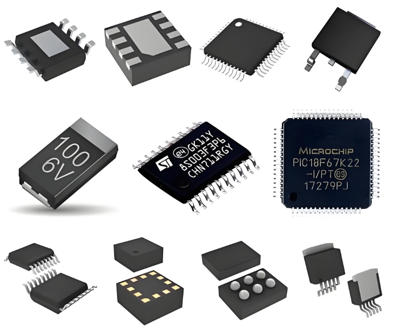
Package: 100-pin Thin Quad Flat Pack (TQFP), a surface-mount package suitable for space-constrained designs.
I/O Count: 64 user I/O pins.
Voltage: 3.3V core voltage with 3.3V or 2.5V I/O operation.
In-System Programmability (ISP): The "isp" in ispMACH signifies that the device can be programmed and reprogrammed directly on the circuit board via a standard 4-wire JTAG (IEEE 1149.1) interface, simplifying both prototyping and field upgrades.
Instant-On: The configuration is stored in non-volatile E²CMOS® cells. This allows the device to become operational microseconds after power-up, a critical feature for system control and initialization sequences.
Primary Application Domains

The deterministic timing and non-volatile nature of the LC4256V-75TN100C make it ideal for "glue logic" and system management tasks, including:
Address Decoding and Bus Interface: Acting as a bridge between processors and peripherals with different bus standards.
State Machine Control: Implementing complex, high-speed control algorithms for system management.
Data Path Control and Routing: Managing the flow of data between different functional blocks.
Power-Up Sequencing and System Configuration: Utilizing its instant-on feature to configure other devices in the system, such as FPGAs and ASICs, immediately upon power application.
I/O Expansion and Aggregation: Consolidating numerous discrete logic ICs into a single, programmable device to reduce board space and component count.
Design and Development
Development for the LC4256V-75TN100C is supported by Lattice's design software suite, now part of the Lattice Radiant® toolchain. Designers use Hardware Description Languages (HDLs) like VHDL or Verilog to describe the logic, which is then synthesized, placed-and-routed, and timing-analyzed for the target device. The predictable timing model significantly simplifies the process of achieving timing closure compared to more complex FPGAs.
ICGOODFIND Summary
The Lattice LC4256V-75TN100C is a robust and reliable CPLD that excels in applications requiring predictable timing, high performance, and instant-on operation. Its 256-macrocell capacity and 64 I/O pins in a TQFP-100 package make it a versatile choice for system integration, control logic, and bridging functions. While newer, more dense programmable logic devices exist, the LC4256V remains a relevant and powerful solution for a vast range of embedded and digital design challenges where its core CPLD advantages are essential.
Keywords:
1. CPLD (Complex Programmable Logic Device)
2. Predictable Timing
3. Instant-On
4. In-System Programmability (ISP)
5. Generic Logic Block (GLB)
